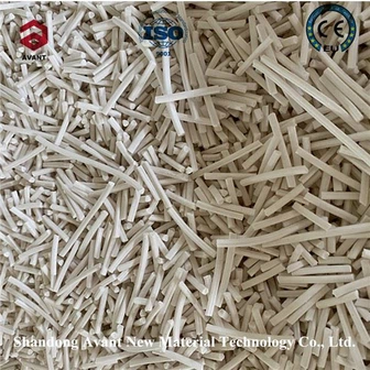
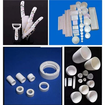
Ceramic Substrate Preparation Technology
According to the packaging structure and application requirements, ceramic substrates can be divided into two categories: planar ceramic substrates and three-dimensional ceramic substrates.
And according to different preparation principles and processes, flat ceramic substrates can be divided into thin-film ceramic substrates (TFC), thick-film printed ceramic substrates (TPC), direct bonded copper ceramic substrates (DBC), active metal welded ceramic substrates (AMB), direct Electroplated copper ceramic substrate (DPC) and laser activated metal ceramic substrate (LAM), etc.
1. Thin Film Ceramic Substrate (TFC)
TFC uses thin film processes such as magnetron sputtering, vacuum evaporation and electrochemical deposition to form metal layers on the surface of ceramic substrates, and then forms specific metal patterns through processes such as masking and etching.
The process has low working temperature, high wiring precision, controllable metal layer thickness and high bonding strength between metal ceramics. The ceramic substrate materials commonly used in thin film technology mainly include Al2O3, AlN and BeO.
Thin-film ceramic substrates are mainly used in device packaging with low current, small size, high heat dissipation requirements, and high wiring accuracy requirements.

2. Thick film printing ceramic substrate (TPC)
TPC uses the screen printing process to print the metal wiring layer, the preparation process is simple, the requirements for processing equipment and environment are low, and it has the advantages of high production efficiency and low manufacturing cost.
However, due to the limitation of the screen printing process, the TFC substrate cannot obtain high-precision circuits. In addition, in order to reduce the sintering temperature and improve the bonding strength of the metal layer and the ceramic substrate, a small amount of glass phase is usually added to the metal paste, which will inevitably reduce the Electrical and thermal conductivity of metal wiring layers.
Therefore, thick-film printed ceramic substrates are only used in electronic device packaging that does not require high circuit accuracy, such as automotive electronic packaging.

3. Direct Bonded Copper Ceramic Substrate (DBC)
The DBC ceramic substrate is heated in nitrogen containing oxygen at a high temperature above 1000 °C, so that the copper foil and the ceramic substrate are firmly bonded together by eutectic bonding, which has high bonding strength and good thermal conductivity. and thermal stability.
Widely used in insulating bipolar diodes, lasers, focusing photovoltaics and other device packaging and heat dissipation.

4. Active Metal Bonded Ceramic Substrate (AMB)
The AMB ceramic substrate is a further development of the DBC process. This process realizes the connection between the ceramic substrate and the copper foil through the solder containing a small amount of rare earth elements, and has high bonding strength and good reliability. Compared with the DBC process, this process has a lower bonding temperature and is easier to operate.
The preparation process flow is as follows:

5. Direct Electroplating Copper Ceramic Substrate (DPC)
The DPC ceramic substrate uses laser to punch holes on the ceramic substrate, uses a semiconductor process to deposit a Cu seed layer on the ceramic substrate, and fills the holes through an electroplating process to thicken the metal layer. This process has the characteristics of high circuit precision and low preparation temperature.
This process enables vertical interconnection of ceramic substrates to increase packing density. The disadvantage is that the metal circuit layer is prepared by the electroplating process, which pollutes the environment, the electroplating growth rate is low, the thickness of the circuit layer is limited, and it is difficult to meet the packaging requirements of high-current power devices. DPC ceramic substrates are mainly used in high-power LED packaging.
The preparation process flow is as follows:

6. Laser Activated Cermet Substrate (LAM)
The LAM ceramic substrate is heated by a laser beam to activate the surface of the ceramic substrate to be metallized, and then metallized wiring is formed by electroplating or electroless plating.
This process does not require micro-machining processes such as photolithography, development, and etching. The circuit layer is prepared by direct laser writing, and the line width is determined by the laser spot, with high precision. The circuit layer can be prepared on the surface of three-dimensional structural ceramics, breaking through the traditional flat ceramics. Limited by the metallization of the substrate, the bonding strength between the metal layer and the ceramic substrate is high, the surface of the circuit layer is flat, and the roughness is at the nanometer level.
However, it is difficult to mass-produce and the price is extremely high, and it is currently mainly used in the aerospace field.